Article Index
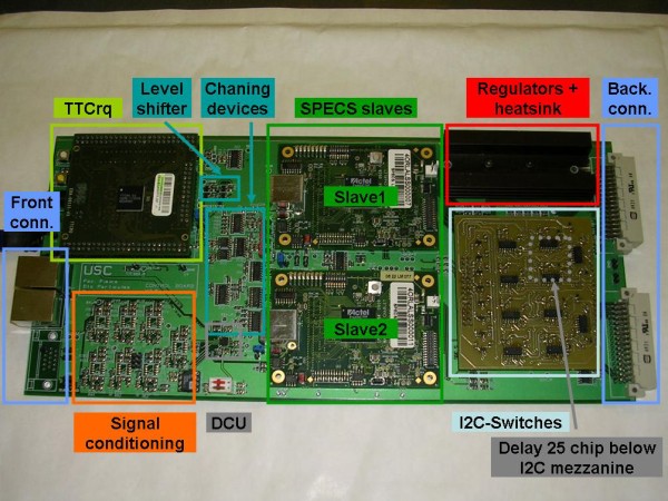
- Power Regulators: 3 LHC491387[3] power regulators for supplying the 2.5V, 3.3V and 5V needed by the CB devices.
- Frontal and backplane connectors:
-
The frontal connectors consist of:
-
1 SubD high density connector for the detector box environmental monitoring.
-
RJ45 connectors for the SPECS[1] chain connection.
-
An AMP/Tyco 6 pin row connector for monitoring the IT half station position switches.
-
-
The backplane connectors are 2 half size DIN 41612
-
- TTCrq: the TTCrq[2] is mezzanine card developed by the CERN microelectronics group containing the TTCrx and other associated components such as a pin-preamplifier and a QPLL.
-
TTCrx: An ASIC receiver developed for the LHC Timing, Trigger and Control (TTC)[4] distribution system. The ASIC implements an interface between the front–end electronics and the TTC system making the TTC coding and multiplexing schemes transparent. The receiver delivers the LHC timing reference signal, the first level trigger decisions and its associated bunch and event numbers. It can be programmed to compensate for the propagation delays associated with the detectors and their electronics. The IC supports the transmission of data and of synchronised broadcast commands.
-
A connectorized PIN photodiode with a trans-impedance amplifier for the reception of the TFC signals from the optical TTC network. Radiation tested.
-
QPLL: Phase-Locked Loop based on a Voltage Controlled Quartz Crystal Oscillator (VCXO). Its function is to act as a jitter-filter and clock multiplier for clock signals operating at the LHC bunch-crossing frequency (40.08 MHz). The device is implemented in a 0.25 µm CMOS technology using radiation tolerant layout practices.
-
- Delay25 chip: it is a 5 channel CMOS programmable delay line featuring 4 channels that allow phase delaying of periodic or non-periodic digital signals and a master channel that can be used to phase delay a clock signal. The master channel serves as a calibration reference. The phase of each channel can be independently programmed with a resolution of 0.5 ns through an I2C interface. The reference clock frequency can be any of the following: 32, 40, 64 or 80 MHz.
- SPECS slaves: These are two mezzanine cards[1] hosted in the CB developed for interfacing electronic devices to the Experiment Control System. The SPECS System is composed of a PCI master card (typically located in the control room faraway form the nasty radiation environment) which can address several SPECS slave mezzanines. The heart of the mezzanines is a radiation tolerant FPGA, but it also contains a radiation hard ADC (the DCU) and some radiation tolerant LVDS drivers and receivers for driving the SPECS communication to the master. Three standard interfaces are provided by the SPECS Slave to control the components on the board or at distances of up to 10 meters: I2C, JTAG and a (simple) parallel bus (only directly on the board), from which we only use the I2C.
- SPECS chaining devices: it is a compendium of LVDS drivers and receivers implemented in the CB for chaining many SPECS slaves in the same SPECS master link. This chaining mechanism is both used for interconnecting the 2 SPECS slaves in the CB and also for interconnecting with other CBs.
- Signal conditioning devices: wheatstone bridges and instrumentation amplifiers used for conditioning the temperature and humidity signals.
- DCU: a radiation hard ADC[5] used for sampling the humidity signal and some others.
- I2C bus switches: a mezzanine card whose purpose is demultiplexing the “SPECS fashion” long I2C bus into 8 individual open collector compatible I2C buses. These I2C buses are necessary for controlling all the Beetles in the Detector Boxes and the GOLs and DCUs in the digitizer boards. A detailed description of the partitioning and I2C address assignment is show later.
- Level shifter: it consists of 2 bipolar transistors working in saturation mode [6] which allow for translating the 2.5V I2C generated by the SPECS slave into 3.3V necessary for TTCrq voltage compatibility.

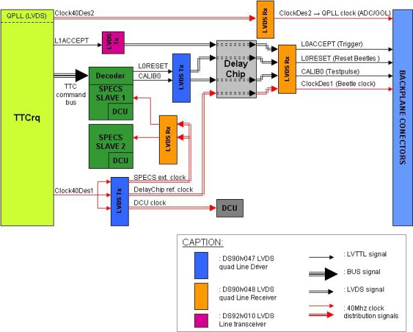
It is also of special interest the clock and TTC signal distribution. The TTCrq delivers the two clocks needed for the Beetles and the sampling electronics (clockDes1 and clockDes2), the trigger signal (L0ACCEPT) and the TTC command bus from which the L0Reset and the calibration signal are decoded. The L0RESET and the TESTPULSE signal (CALIB0) are decoded in the SPECS FPGA and the decoding of the latter can be delayed by the SPECS from 0 to 16 cycles of 25ns. All these signals but the clockDes2 pass through the Delay25 chip so they can be phase delayed within a range of 32ns in steps of 0.5ns, therefore a fine tuning of its timing is possible.

-
-
1 SubD high density connector for the detector box environmental monitoring.
-
RJ45 connectors for the SPECS[1] chain connection.
-
An AMP/Tyco 6 pin row connector for monitoring the IT half station position switches.
-


